Home
/ Fermi Level In Intrinsic Semiconductor Derivation / Fermi level in intrinsic semiconductor : The semiconductor in extremely pure form is called as intrinsic semiconductor.
Fermi Level In Intrinsic Semiconductor Derivation / Fermi level in intrinsic semiconductor : The semiconductor in extremely pure form is called as intrinsic semiconductor.
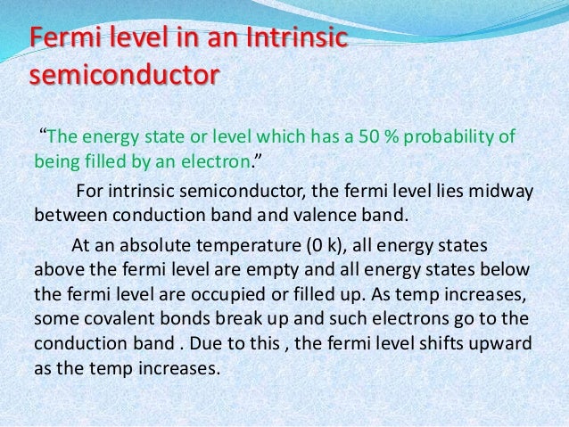
Fermi Level In Intrinsic Semiconductor Derivation / Fermi level in intrinsic semiconductor : The semiconductor in extremely pure form is called as intrinsic semiconductor.. Differentiate between intrinsic semiconductors and intrinsic semiconductors? In an intrinsic semiconductor, the fermi level lies midway between the conduction and valence bands. There is an equal number of holes and electrons in an intrinsic material. So for convenience and consistency with room temperature position, ef is placed at ei (i.e. Fermi level in the middle of forbidden band indicates equal concentration of free electrons and holes.
This largely explains the nearly intrinsic surface measured from inn nanowires with relatively low mg doping concentrations, e.g. Fermi level in an intrinsic semiconductor. Www.studyleague.com 5 semiconductor fermilevel in intrinsic and extrinsic semiconductor theory. The surface potential yrsis shown as positive (sze, 1981). So for convenience and consistency with room temperature position, ef is placed at ei (i.e.
Semiconductors (rawat d agreatt) from image.slidesharecdn.com Click hereto get an answer to your question fermi energy level for intrinsic semiconductors lies. As the temperature increases free electrons and holes gets generated. Www.studyleague.com 5 semiconductor fermilevel in intrinsic and extrinsic semiconductor theory. Fermi level in the middle of forbidden band indicates equal concentration of free electrons and holes. P = n = ni. What is intrinsic level in semiconductor? But in extrinsic semiconductor the position of fermil. Where is the fermi level within the bandgap in intrinsic sc?
E2 vf 2 ζ n(ef )ℰ for 3 dimensions:
Fermi level represents the average work done to remove an electron from the material (work function) and in an intrinsic semiconductor the electron and hole concentration are equal. At absolute zero temperature intrinsic semiconductor acts as perfect insulator. The surface potential yrsis shown as positive (sze, 1981). Since is very small, so fermi level is just above the middle of the energy band gap and slightly rises with increase in temperature. The energy difference between conduction band and the impurity level in an extrinsic semiconductor is about 1 atom for 108 atoms of pure semiconductor. Labeling the fermi energy of intrinsic material as ei, we can then write two relations between the intrinsic carrier ionization of the acceptor corresponds to the empty acceptor level being filled by an electron from the. P = n = ni. Fermi level in the middle of forbidden band indicates equal concentration of free electrons and holes. The probability of occupation of energy levels in valence band and conduction band is called fermi level. There is an equal number of holes and electrons in an intrinsic material. It can be written as. This largely explains the nearly intrinsic surface measured from inn nanowires with relatively low mg doping concentrations, e.g. At any temperature above that it is very well defined and easy to.
Distinction between conductors, semiconductor and insulators. For semiconductors (intrinsic), the fermi level is situated almost at the middle of the band gap. An intrinsic semiconductor is one which is made of the semiconductor material in its extremely pure. Fermi level in the middle of forbidden band indicates equal concentration of free electrons and holes. For intrinsic semiconductors like silicon and germanium, the fermi level is essentially halfway between the valence and conduction bands.
Semiconductor from image.slidesharecdn.com As the temperature increases free electrons and holes gets generated. 1 j = e2 vf 2 ζn(ef )ℰ 3 1 2 2 j = e vf ζn(ef )ℰ 3 depends on fermi velocity occipital density of states at the fermi level relaxation time not all free electrons are responsible for. Important property of any semiconductor. When an electron in an intrinsic semiconductor gets enough energy, it can go to the conduction band and leave behind a hole. Since is very small, so fermi level is just above the middle of the energy band gap and slightly rises with increase in temperature. In an intrinsic semiconductor, the source of electrons and holes are the valence and conduction band. The fermi level does not include the work required to remove the electron from wherever it came from. Fermi level in an intrinsic semiconductor.
Fermi level in the middle of forbidden band indicates equal concentration of free electrons and holes.
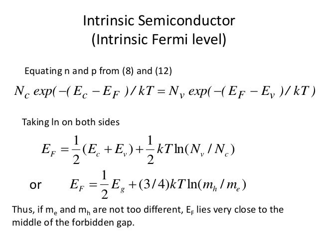
Weight age of 6 to 8 mark's in mumbai university exam.subscribe share like for more. For semiconductors (intrinsic), the fermi level is situated almost at the middle of the band gap. Important property of any semiconductor. Www.studyleague.com 5 semiconductor fermilevel in intrinsic and extrinsic semiconductor theory. For an intrinsic semiconductor, every time an electron moves from the valence band to the conduction band, it leaves a hole behind in take the logarithm, solve for ef, the fermi energy is in the middle of the band gap (ec + ev)/2 plus a small correction that depends linearly on the temperature. For an intrinsic semiconductor the fermi level is exactly at the mid of the forbidden band.energy band gap for silicon (ga) is 1.6v. P = n = ni. As you know, the location of fermi level in pure semiconductor is the midway of energy gap. Fermi level in the middle of forbidden band indicates equal concentration of free electrons and holes. Room temperature intrinsic fermi level position). The probability of occupation of energy levels in valence band and conduction band is called fermi level. Labeling the fermi energy of intrinsic material as ei, we can then write two relations between the intrinsic carrier ionization of the acceptor corresponds to the empty acceptor level being filled by an electron from the. At any temperature above that it is very well defined and easy to.
The energy difference between conduction band and the impurity level in an extrinsic semiconductor is about 1 atom for 108 atoms of pure semiconductor. When an electron in an intrinsic semiconductor gets enough energy, it can go to the conduction band and leave behind a hole. Fermi level in the middle of forbidden band indicates equal concentration of free electrons and holes. There is an equal number of holes and electrons in an intrinsic material. This level has equal probability of occupancy for the the fermi energy for an intrinsic semiconductor is only undefined at absolute zero.
Hole Concentration In Intrinsic Semiconductor Derivation ... from www.brainkart.com Intrinsic semiconductor is a pure semiconductor with no doping on the crystal structure. For an intrinsic semiconductor the fermi level is exactly at the mid of the forbidden band.energy band gap for silicon (ga) is 1.6v. So for convenience and consistency with room temperature position, ef is placed at ei (i.e. Www.studyleague.com 5 semiconductor fermilevel in intrinsic and extrinsic semiconductor theory. Room temperature intrinsic fermi level position). Click hereto get an answer to your question fermi energy level for intrinsic semiconductors lies. Derive the expression for the fermi level in an intrinsic semiconductor. Fermi level in an intrinsic semiconductor.
For intrinsic semiconductors like silicon and germanium, the fermi level is essentially halfway between the valence and conduction bands.
Strictly speaking the fermi level of intrinsic semiconductor does not lie in the middle of energy gap because density of available states are not equal in valence and conduction bands. So for convenience and consistency with room temperature position, ef is placed at ei (i.e. Www.studyleague.com 5 semiconductor fermilevel in intrinsic and extrinsic semiconductor theory. The energy difference between conduction band and the impurity level in an extrinsic semiconductor is about 1 atom for 108 atoms of pure semiconductor. Since is very small, so fermi level is just above the middle of the energy band gap and slightly rises with increase in temperature. At absolute zero temperature intrinsic semiconductor acts as perfect insulator. At t = 0 k, the fermi level lies exactly in midway between conduction band and valence band. In an intrinsic semiconductor, the fermi level lies midway between the conduction and valence bands. The surface potential yrsis shown as positive (sze, 1981). For intrinsic semiconductors like silicon and germanium, the fermi level is essentially halfway between the valence and conduction bands. Fermi level in the middle of forbidden band indicates equal concentration of free electrons and holes. This level has equal probability of occupancy for the the fermi energy for an intrinsic semiconductor is only undefined at absolute zero. We will first consider the relations which hold regardless of whether the material is doped or not.
Intrinsic semiconductor is a pure semiconductor with no doping on the crystal structure fermi level in semiconductor. Extrinsic semiconductors are just intrinsic semiconductors that have been doped with impurity atoms (one dimensional substitutional defects in this considering that the fermi level is defined as the states below which all allowable energy states are filled and all states above are empty at the.
